PADS Layout Translate: Essential Tips for PCB Designers 5 common mistakes pcb designers should avoid • ecadstar
If you are looking for Can AI Truly Replace Human PCB Designers? you've visit to the right place. We have 25 Pictures about Can AI Truly Replace Human PCB Designers? like PCB Trace Basics For PCB Designers | Reversepcb, Can AI Truly Replace Human PCB Designers? and also Can AI Truly Replace Human PCB Designers?. Here you go:
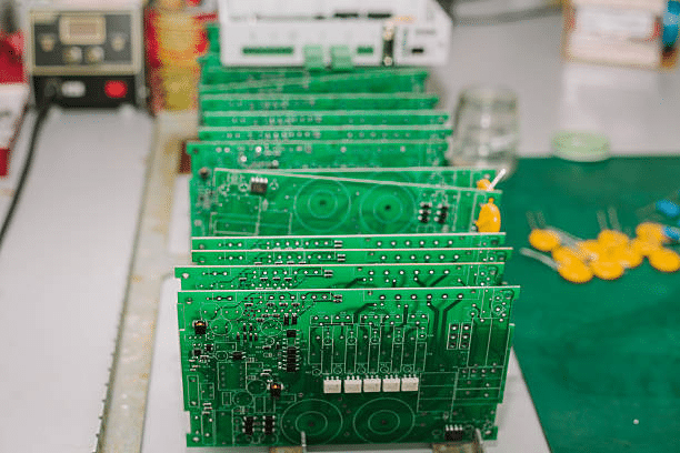
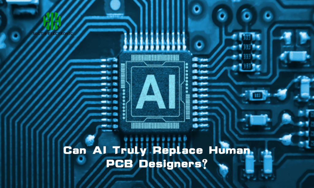
Can AI Truly Replace Human PCB Designers?
 southelectronicpcb.com
Can AI Truly Replace Human PCB Designers?
Layout Translate Stock Illustrations – 1,073 Layout Translate Stock
 www.dreamstime.com
Layout Translate Stock Illustrations – 1,073 Layout Translate Stock ...
Demystifying Standard FR4 Thickness: A Comprehensive Guide For PCB
 ksnpcb.com
Demystifying Standard FR4 Thickness: A Comprehensive Guide for PCB ...
Layout Translate Stock Illustrations – 1,073 Layout Translate Stock
 www.dreamstime.com
Layout Translate Stock Illustrations – 1,073 Layout Translate Stock ...
Pads Layout Viewer Download: The Key To Streamlining Your PCB Design
 www.raypcb.com
Pads Layout Viewer Download: The Key to Streamlining Your PCB Design ...
PCB Trace Basics For PCB Designers | Reversepcb
 reversepcb.com
PCB Trace Basics For PCB Designers | Reversepcb
Why 98% Of Successful Pcb Designers Prioritize Effective Pcb Layout
 gighz.net
Why 98% of successful pcb designers prioritize effective pcb layout ...
Can AI Truly Replace Human PCB Designers?
 southelectronicpcb.com
Can AI Truly Replace Human PCB Designers?
Pads Layout Viewer Download: The Key To Streamlining Your PCB Design
 www.raypcb.com
Pads Layout Viewer Download: The Key to Streamlining Your PCB Design ...
Focus On Embedded Development For PCB Designers | Altium
 resources.altium.com
Focus on Embedded Development for PCB Designers | Altium
Pros And Cons Of Advanced Electronic Packaging For PCB Designers
Pros and Cons of Advanced Electronic Packaging for PCB Designers ...
PCB Designers Share Their Experience In PCB Design With BGA Devices
 www.kingfordpcb.com
PCB designers share their experience in PCB design with BGA devices ...
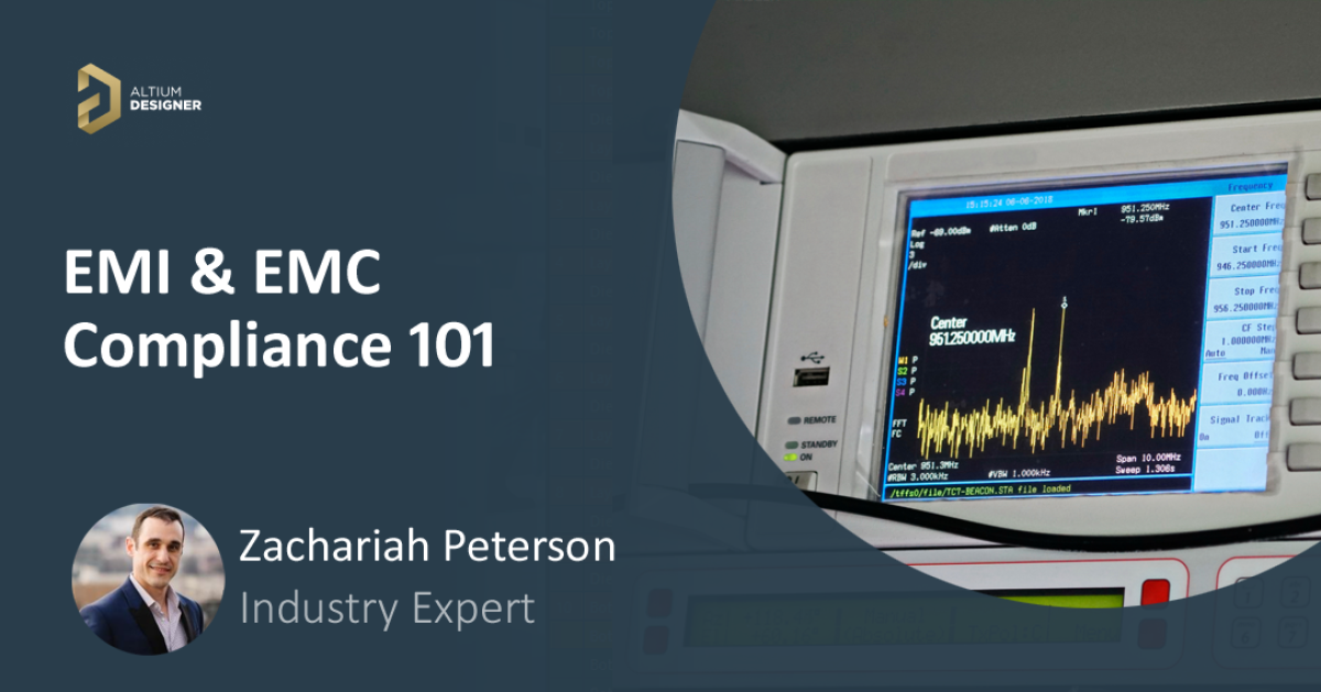
EMI And EMC Compliance 101 For PCB Designers
 resources.altium.com
EMI and EMC Compliance 101 for PCB Designers
5 Essential Portfolio Tips For Designers
 www.linkedin.com
5 Essential Portfolio Tips For Designers
The Essential Role And Impact Of PCB Designers In The World Of
 engineering.soldered.com
The Essential Role and Impact of PCB Designers in the World of ...
5 Common Mistakes PCB Designers Should Avoid • ECADSTAR
 www.ecadstar.com
5 Common Mistakes PCB Designers Should Avoid • eCADSTAR
PCB Designers PCB Circuit Board Assembly Wireless Charger PCBA - China
 newchip.en.made-in-china.com
PCB Designers PCB Circuit Board Assembly Wireless Charger PCBA - China ...
Spanish PCB Design Landscape: University Origins & Regional Demand Trends
 www.linkedin.com
Spanish PCB Design Landscape: University Origins & Regional Demand Trends
The Essential Role And Impact Of PCB Designers In The World Of
 engineering.soldered.com
The Essential Role and Impact of PCB Designers in the World of ...
Collaboration For Mechanical & PCB Designers | Guides | Altium 365
 resources.altium365.com
Collaboration for Mechanical & PCB Designers | Guides | Altium 365
Basics For Pdn Pcb Designers | PDF
 www.slideshare.net
Basics for pdn pcb designers | PDF
Antenna Design Principles For PCB Designers
 www.linkedin.com
Antenna Design Principles for PCB Designers
Podcast: PCB 3.0: SI/PI For PCB Designers - System, PCB, & Package
 community.cadence.com
Podcast: PCB 3.0: SI/PI for PCB Designers - System, PCB, & Package ...
PCB Designers To Contest For Design Champion Title At IPC APEX EXPO 2024
 www.pcbdirectory.com
PCB Designers to Contest for Design Champion Title at IPC APEX EXPO 2024
Essential Information And Tips For Using Taconic PCB
 pcbassemblymanufacturing.com
Essential information and tips for using Taconic PCB
pads layout viewer download: the key to streamlining your pcb design .... Emi and emc compliance 101 for pcb designers. Pcb designers pcb circuit board assembly wireless charger pcba